
In the previous post, we learned how 3D NAND increased the areal density of Flash memory by employing geometrical, structural and material based innovations. As a result, it is 10x denser and 1000x faster than traditional NAND. However, it is uncertain if we can continue pushing the limits of NAND Flash. The obstacles are not only technical but also economic: the very viability of NAND Flash is being questioned due to high manufacturing costs. This has led researchers to look at alternative technologies. Phase Change Memory (PCM), a very promising technology, is one of the many options that are being actively researched. We will briefly examine the advantages and limitations of PCM In this post.
Advantages of PCM over DRAM and NAND Flash
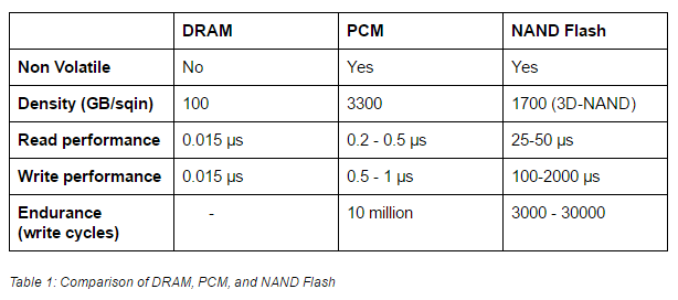
As shown in tabIe 1 below, PCM has several advantages over DRAM and NAND Flash. Unlike DRAM, PCM does not lose data when powered off. It also has a significantly higher areal density than DRAM. Similarly, if we compare PCM with NAND Flash, it beats the latter, both in performance and endurance. Moreover, PCM’s ability to store 3 bits per cell can push its cost lower than DRAM and bring it close to the NAND Flash range.
PCM sits somewhere between DRAM and NAND Flash on most comparison metrics. One might be tempted to think that PCM could replace both in the future, but according to Haris Pozidis, manager of non-volatile memory research at IBM Research – Zurich, PCM’s true potential is not in replacing DRAM or NAND Flash, but in complementing both.
Speaking at this week’s IEEE International Memory Workshop in Paris, Pozidis said he doesn’t envision PCM as a replacement for DRAM or NAND flash technologies. But he said it could “fill a void between the two” and enable and accelerate applications such as in-memory databases or big-data, machine-learning applications. –– IBM claims breakthrough with TLC phase change memory
A peek into PCM’s technology
A PCM cell is made of Chalcogenide glass, an alloy of various elements. Chalcogenide glass exhibits two stable states with different electrical resistance: amorphous and crystalline, which can encode the boolean states of ‘0’ and ‘1’ to implement a 1-bit cell.
Data is written to a PCM cell by applying a current pulse through a heating element generally made of TiN. The electric current brings the glass close to its molten state, after which the glass subsequently settles into either a crystalline or amorphous state depending on the rate at which it is cooled. If it’s cooled gradually with a long, low-intensity current pulse, then it becomes crystalline. Alternately, if the glass is heated by a short, high-intensity current pulse, the surrounding cold material subsequently quenches the hot region, making it amorphous.
Data is read back using the cell’s resistance as an indicator since the amorphous state is characterized by high resistance and the crystalline state with low resistance¹.
Multi-bit cells: The team at IBM researching PCM found something very interesting. They found that even though Chalcogenide glass supports only two stable states (amorphous and crystalline), it supports several stable resistance thresholds. This has a very important implication for PCM’s areal density because a cell with four stable thresholds can encode two bits and a cell with eight thresholds can encode three bits. The current state of PCM technology supports 3-bit cells.
However, implementing multi-bit cells has not been without challenges. The amorphous state of Chalcogenide glass is not quite stable. It’s resistance increases with time as its atoms gradually rearrange themselves towards the more stable crystalline state. This phenomenon, known as resistance drift, can result in data corruption if not compensated. According to the scientists at IBM, technical advancements were needed both in the read as well as write states to rectify the problem of resistance drift.
A technique called iterative writing was used to overcome issues in writing data:
The scientists implemented an iterative “write” process to overcome deviations in the resistance due to inherent variability in the memory cells and the phase-change materials: “We apply a voltage pulse based on the deviation from the desired level and then measure the resistance. If the desired level of resistance is not achieved, we apply another voltage pulse and measure again — until we achieve the exact level,” explains Pozidis. — IBM scientists demonstrate computer memory breakthrough
And the issues in reading were overcome by using drift tolerant coding and detection schemes:
For demonstrating reliable read-out of data bits, the scientists needed to tackle the problem of resistance drift. Because of structural relaxation of the atoms in the amorphous state, the resistance increases over time after the phase change, eventually causing errors in the read-out. To overcome that issue, the IBM scientists applied an advanced modulation coding technique that is inherently drift-tolerant. The modulation coding technique is based on the fact that, on average, the relative order of programmed cells with different resistance levels does not change due to drift. — IBM scientists demonstrate computer memory breakthrough
Challenges and the road ahead
One of the biggest challenge that PCM faces today is the gap between the promised speed and what has been actually attained. The Non-Volatile Systems Laboratory in the University of California at San Diego (UCSD), built a prototype PCI-attached PCM drive to study various aspects of this new technology. Their results show that the current performance of PCM is a far cry from what was promised.
The PCM SSDs were only seven times faster than single-level cell (SLC) flash-based SSDs for small data requests of less than 8 KB, and up to 30{00650960c7c98e0cfb19b413dfe1b11628fd22333dea5da8eda402d86148a18a} faster for larger data requests. In some cases, the PCM SSDs were even 50{00650960c7c98e0cfb19b413dfe1b11628fd22333dea5da8eda402d86148a18a} slower than SLC flash with data requests of more than 8 KB, according to Swanson.
He [Swanson] said these results were a far cry from PCM projections of 50,000 times faster than disk and 1,000 times faster than flash. — UCSD lab studies future changes to non-volatile memory technologies
According to Swanson, the gap in performance comes from slow NOR like interfaces used in PCM chips and the slow speed of transition between crystalline and amorphous states. However, he also adds that both these problems will be addressed as the technology matures. The chip’s current NOR like interface is likely to evolve into something closer to what is used in conventional memory; consequently, reducing the interface bottleneck. The slow transition speed of the metal alloy which is attributed to its large cell size will also improve when the size of the cell is reduced.
In the next post we will discuss another non-volatile memory technology called memristors. Similar to PCM, memristors also offer performance gains and better endurance as compared to Flash NAND. However, the endurance promised by memristors is significantly higher than PCM and they also have the added advantage of lower power consumption.
Footnotes:
- Newer PCM technology has been trending in two different directions. One group has been directing a lot of research towards attempting to find viable material alternatives to Ge2Sb2Te5 (GST), with mixed success. Another have developed the use of a GeTe – Sb2Te3 superlattice to achieve non-thermal phase changes by simply changing the coordination state of the Germanium atoms with a laser pulse. This new Interfacial Phase Change Memory (IPCM) has had many successes and continues to be the site of much active research. — https://en.wikipedia.org/wiki/Phase-change_memory