
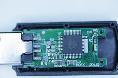
Image by Pascal Volk, licensed under CC BY-SA 2.0
Storage technology is a subject that is very close to my heart. I discussed Hard Disk Trends about a year ago and was fascinated by what I learned in my survey. This time, I’d like to share what I am learning about Non-Volatile Memory (NVM). This is the first in a series of posts on Non-Volatile Memory which present an ‘under the hoods’ peek at the technology that powers those wonderful devices.
Although Non-Volatile Memory only has a history of approximately thirty years, about twenty years less than its hard disk cousin, it too has been evolving exponentially since its commercial beginnings.
I’d like to begin this series with a discussion on basic technical concepts related to the current state of this technology. After that, we will look at a few limitations for maintaining the growth trajectory that this technology has enjoyed over the past several years. The rest of the series will discuss technological innovations that promise to support a similar growth story for Flash for some more time to come.
Non-Volatile Memory Designs
The first commercially viable form of NVM was called Flash Memory. Flash was built from floating gate MOSFET silicon transistors which have the capability to hold charge (electrons) in an electrically isolated region called a floating gate that can be probed to detect its state.
Flash can be manufactured using either NOR or NAND gates, and independently, it can also be designed for one or more logical bits per cell. We’ll discuss these variations below.
NOR or NAND
Most of you must be familiar with NOR and NAND gates. Flash can be built with either of them, but the latter is more popular because of its endurance and higher density. However, despite its advantages, NAND flash also has certain limitations.
The first limitation is Block Erasure, which means, cells containing zeroes cannot be overwritten at byte or word level. Instead, an entire block of data has to be first erased using an erasure procedure that sets all bits of the block to one. Subsequently, a one-to-zero bit transition can be performed at byte level.
Read disturb is another issue associated with NAND Flash. The process of reading cells several times can affect the charge of an otherwise untouched adjacent cell. To avoid data corruption after a certain number of read cycles, the data block is copied to another block before its data has degraded to the point of irrecoverability.
Yet another drawback of NAND Flash is Memory Wear. High voltages used in the erasure cycle cause gradual physical degradation of the cells. After a certain number of such erasures, a block loses its ability to store data. Current flash technologies can withstand 105 – 106 erase cycles.
Notwithstanding these drawbacks, NAND flash has been a resounding success due to its low price per GB. It’s used everywhere from cell phones to laptops to enterprise data centers.
Single Level or Multiple Level
Flash Memory holds data in cells which can store one or more bits depending on how they are designed. Single Level Cells (SLC) support 1 bit/cell, Multiple Level Cells (MLC) support 2 bits/cell, and Triple Level Cells (TLC) support 3 bits/cell. Attempts are successfully being made to go beyond TLC; although, as this article puts it, it’s tricky to get the right balance of performance and density in Quad Level Cells (QLC) which encode 4 bits/cell.
At present, both SLC and MLC are in use, although for somewhat different usage requirements. MLC/TLC show up more in consumer goods since their per GB cost is less than SLC. SLC have higher performance; so they tend to be seen in enterprise class devices.
Moore’s Law and Flash
Much of what we have discussed until now may be common knowledge to those who are familiar with Flash technology. However, an interesting point that emerges is that Flash technology has begun to run into fundamental limits. As memory cells shrink in size, the number of electrons representing one bit has been reduced to about 50-100. When a cell has only so many electrons it becomes susceptible to more leakage and disturbance from nearby cells. Reduced reliability of cells results in a need to add redundant cells for error correction, defeating the purpose of reducing cell size. We’ve probably hit a spot where reducing cell size (using the current technology) will not have any significant impact on reducing the size of the overall media. A question that many people have started asking is: will Moore’s law continue to hold up for Flash memory areal densities over the next couple decades?
Up till now, flash memory areal densities have followed Moore’s law not only through improvement in processes and materials but also through design innovations. But as we saw earlier, attempts to further shrink the memory cell may be running up against fundamental physical limits. So, is Moore’s law finally running out of steam for Flash? Maybe, or maybe not! In the next few posts, we will look at some recent and future technologies that could allow Moore’s law to continue for some more time.